Modifying a Master System cartridge for use with flash ROMs
Thursday, 22nd August 2019
I have a ToToTEK GG-PRO flash cartridge to run homebrew software on my Game Gear however I have never been able to get it to work on my current PC and it seems that it's hard to find a Master System equivalent these days. A contemporary alternative is the Master EverDrive and it is by all accounts an excellent piece of equipment however it is a very expensive product.
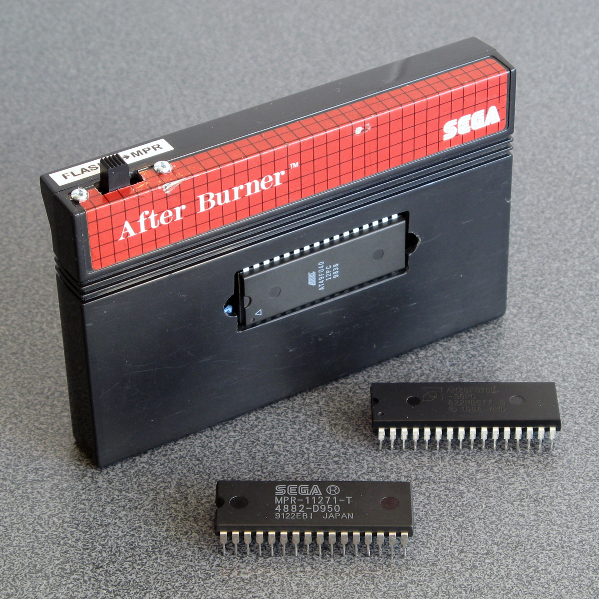
I had, however, heard that certain Master System cartridges could be modified to accommodate a flash memory chip in place of their stock mask ROM. I do say certain cartridges as it's the ones with separate mapper chips that need to be used. One such cartridge is After Burner, and as I was able to find an inexpensive loose copy on eBay I used that as the basis of my modifications.
The memory mapper is used to map ROM banks or save RAM on the cartridge into one of three 16KB slots in the Z80's address space. Most Master System cartridges only contain a single chip that combines the ROM data for the game as well as the memory mapper logic. As such, these cartridges can't be modified for use with a generic flash memory chip as you can't access that internal memory mapper. Some cartridges, however, make use of a separate mapper chip and so you can remove the plain mask ROM chip and replace it with a flash memory chip. SMS Power! has this list of mappers and examples of cartridges in which they can be found.
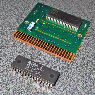
In the photo above you can see where I removed the mask ROM from the cartridge PCB and have left the mapper chip on the board. I didn't want to damage the old ROM chip (in case I wanted to play After Burner again) so I carefully unsoldered it rather than cutting it off the board. To do so I heated up each solder joint on the back of the board and used my spring-loaded solder sucker to remove the molten solder. After this I checked each pin by gently trying to move it in its hole; if it moved I knew it had been unsoldered and if it was stuck fast I knew I needed to try removing more solder. Once all pins were free the old ROM lifted cleanly out of the PCB.
One of convenient features of these cartridges is that the pinout of Sega's mask ROMs is virtually identical to the pinout of commonly-available flash memories like the 29F010 or 49F040. Only two pins need to be changed, as per the information on Charles MacDonald's website:
| Pin | Mask ROM | Flash memory |
|---|---|---|
| 1 | Not connected | A18 |
| 31 | A18 | /WE (Write Enable) |
As I wanted to ensure that the cartridge was compatible with both the original mask ROM and the replacement flash memory chip I thought it best to install a switch to let me select the type of memory that is installed. To break the connection between the solder pad on the PCB and the leg on the memory chip I used an IC socket with legs 1 and 31 bent out and not soldered through their corresponding holes. Wires are soldered to the bent out legs and go via the switch to the corresponding solder pads on the bottom of the PCB.
The position of A18 definitely needed to be swapped between pin 31 on the mask ROM and pin 1 on the flash memory if I wanted to be able to address all 512KB of a 4 megabit ROM. I had heard reports that the write enable pin on the flash memory can be left disconnected however the datasheets for the flash memory chips I checked did seem to indicate that it should be held high during read operations so I thought it best to hold it high when in "flash" mode. This means that the function of both pins needed to be changed by the switch, so I used a DPDT to make this happen. The two different states are illustrated below, showing the connections to the six pins on the bottom of the switch:
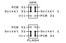
The heavy black lines show the position of the switch contacts when in the upper and lower positions. When in "MPR" mode you can see that pin 31 of the IC socket (A18) is connected to pin 31 of the PCB and pin 1 (NC) of the IC socket is not connected to anything. When in "FLASH" mode pin 31 of the IC socket (now /WE) is connected to Vcc and pin 1 of the IC socket (now A18) is connected to pin 31 of the PCB.
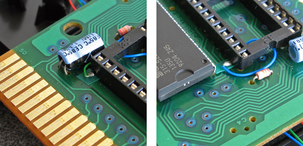
The photos above show how the pins of the IC socket were bent outwards with very fine wires soldered to them. These fine wires run through holes on the PCB under the IC socket to the underside. I did stick very small pieces of electrical insulating tape under the points where the solder joints for the wires attached to the bent pins made contact with the PCB for a bit of added security. With those legs bent out and the wires threaded through the PCB the socket could be soldered down.
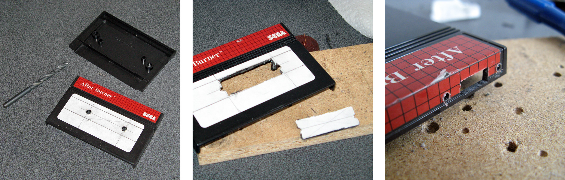
Unfortunately, one problem with using an IC socket is that the extra height means that the PCB no longer fits inside the cartridge shell. I needed to cut a rectangular hole in the cartridge enclosure for the chip to protrude through. I started by drilling two large round holes at the far ends of the chip - this allows me to use a chip puller (or small screwdriver) to pull (or lever) the chip out of the socket without needing to dismantle the cartridge each time. Due to the position of an internal support post very near to the memory chip a larger rectangular slot could not be cut – and I think this looks pretty neat anyway! A smaller rectangular hole was cut in the top of the cartridge shell for the switch to protrude through along with mounting holes for its two screws.
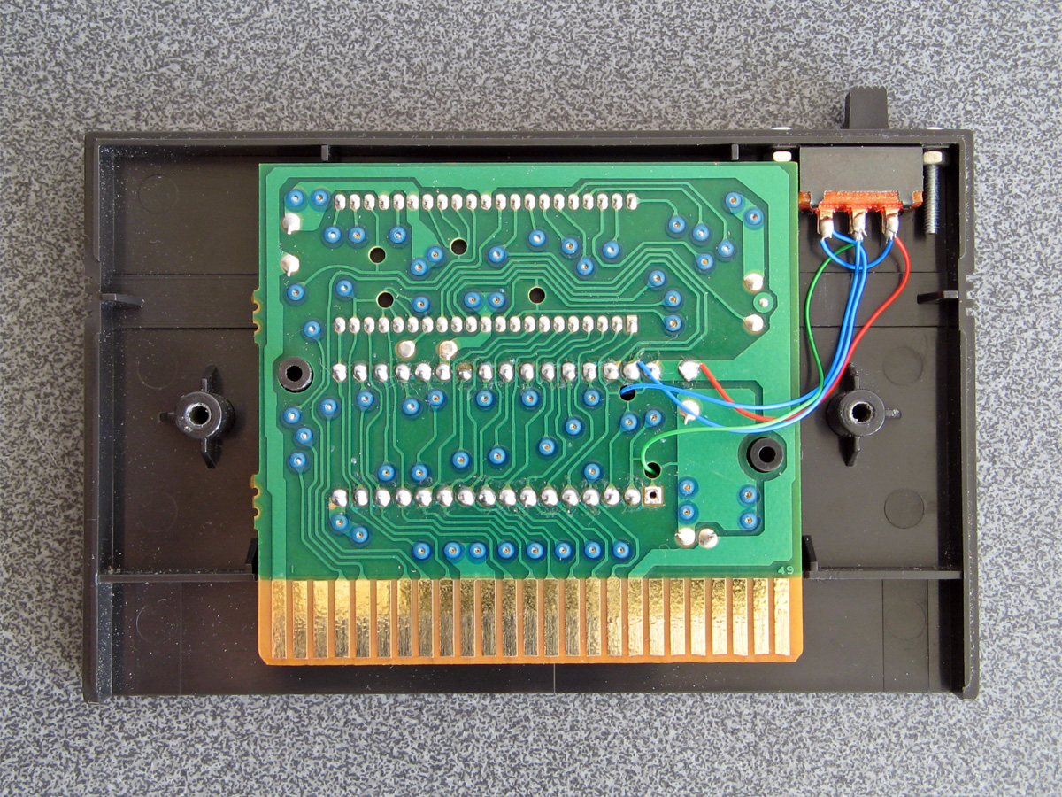
Here the switch has been mounted inside the case with the wires from the IC socket soldered to the appropriate pins on the switch and other wires connected to the appropriate pads on the back of the back of the PCB.
Inserting the original mask ROM for After Burner and setting the switch to MPR mode lets me play After Burner; writing a ROM image to a flash memory chip and inserting that with the switch set to FLASH mode let me run that program instead. Putting the switch on the wrong mode would take me to the console's built-in game of Hang On as the BIOS is no longer able to read the cartridge as a valid Master System game (at least when using a 512KB memory that requires A18 to be connected to the right pin). All in all I'm now happy that I have a way to run programs on my Master System from flash memory and do some homebrew experiments of my own on real hardware.
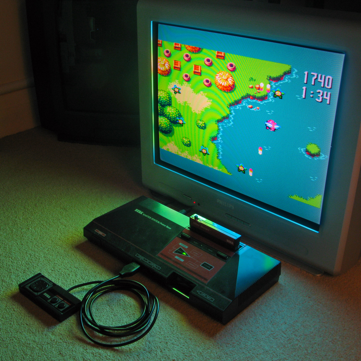
The above photo shows the excellent homebrew Flight of Pigarus by Kagesan running on my Master System courtesy of the modified cartridge. I've tested it so far with an AM29F010B (128KB/1 megabit) and an AT49F040 (512KB/4 megabit) and have been using the Willem programmer (along with Remapped IO.DLL to get it to work with my PC's PCI parallel port) to program the chips.