Booting CP/M 3 from an SD card
Wednesday, 23rd June 2010
Up to this point I have been running CP/M 2.2 on the Z80 computer. CP/M 3 adds a number of useful features, including the following:
- Support for more than 64KB RAM via banked memory.
- Standardised access to real-time clock for file date and time stamping.
- Improved text entry on the command-line when using the memory-banked version, such as the ability to move the cursor when editing and recall the previously entered line.
- Support for disks with physical sectors larger than the default record size of 128 bytes.
Switching to a banked memory system would require some new hardware in the form of a memory management unit so I have stuck with the simpler non-banked system for the time being. Support for physical disk sectors larger than 128 bytes is more interesting (SD cards use 512 byte "blocks") and real-time clocks are always useful so I have started working on updating to CP/M 3.
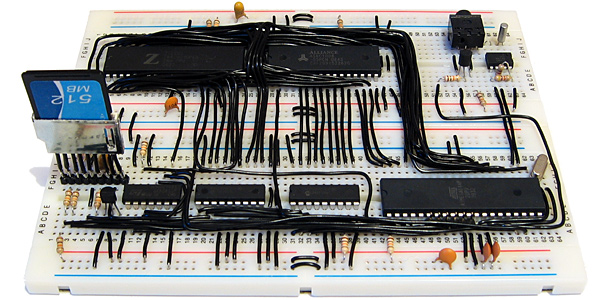
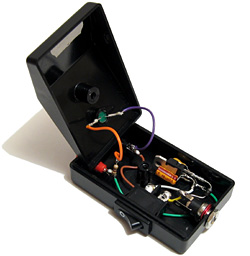
Z80 computer with new SD card slot (bottom left) and real-time clock (top right)
CP/M consists of three main pieces of software:
- A BIOS which exposes a small number of routines to perform primitive, hardware-specific operations (e.g. output a character to the console, read a raw sector from a disk, check if a key has been pressed).
- The BDOS which provides the main API for transient programs (e.g. read a complete line of input from the console, create a file, read a record from a file).
- The CCP, or console command processor, which provides the main user interface for loading and running other programs or performing some basic tasks via its built-in commands. This would be analogous to COMMAND.COM on DOS.
When working with CP/M 2.2 I had source files for these three pieces of software, so I just needed to implement the 17 BIOS functions, reassemble the three files to fixed addresses in memory and load them to these fixed addresses using the AVR when booting the computer. These three files were stored in the lower 8KB of the flash memory chip and were not accessible from within CP/M itself.
CP/M 3 proved to be a bit more of a challenge, as it is loaded slightly differently. The CCP is stored as a regular file named CCP.COM on the floppy disk you're booting from, so only the BIOS and BDOS need to be loaded from their hiding place at the start of the boot disk. These two pieces of software are merged into a single file named CPM3.SYS by a CP/M utility named GENCPM. To get this utility to work I needed to provide GENCPM with a hardware-specific BIOS3.SPR file that implemented the 31 BIOS routines. Fortunately, a file named BIOSKRNL.ASM is provided that implements most of the boilerplate code involved with writing a BIOS (you still have to provide the hardware-specific routines yourself, but your task is made much easier by following the template) so I just needed to recompile that for a non-banked system and link it with my handful of hardware-specific routines.
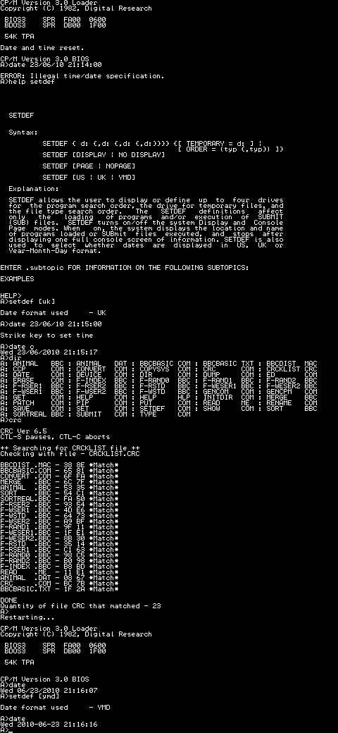
Ideally, CPM3.SYS would be stored on the regular file system with CCP.COM and the hidden boot loader would load CPM3.SYS for you. CP/M 3 does provide a small boot loader for this purpose (aptly named CPMLDR) which employs a cut-down BDOS and BIOS to load CPM3.SYS from the file system into memory for you. I haven't been able to get it to work, though, so I currently parse and load CPM3.SYS using some C code on the AVR. This works well enough for the time being, as can be seen in the above output generated by the computer when testing the real-time clock.
The time and date is maintained by a DS1307, an inexpensive eight-pin real-time clock and calendar chip that is shown in the middle of the above photograph. It is accessed over the I2C bus using a protocol that is natively supported by the AVR hardware. It uses binary-coded decimal to represent dates and times, which corresponds nicely to the time format used by CP/M; however, CP/M represents dates as a 16-bit integer counting the number of days since the 31st December 1977. I have used the algorithms on this website to convert dates to and from this format and the individual components.
The only downside of the DS1307 is that it only stores a two-digit year number, not the four digits one would hope for. This means that the century is discarded when setting the real-time clock, allowing for you to set a date that is then retrieved differently (truncated to the range 1930..2029). I haven't thought of a suitable solution to this problem just yet. I could use the AVR to act as the real-time clock, but I would then lose the advantage of the DS1307's battery backup that kicks in when the main power supply is removed.
The state of the DS1307 is effectively random at power-up. One of the first things the computer does when booting is to read the current date and time and check that all fields are within range. If not it resets them to midnight on the 1st January 1978 and displays a message to indicate that it has done so.
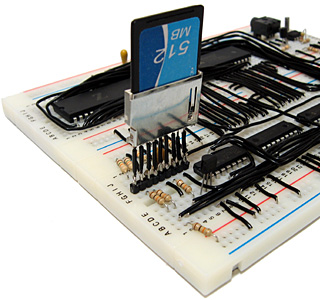
The SD card has been a bit of a headache to get working and though it currently only supports reading, not writing, it should hopefully be a useful addition to the computer. Rather than the previous arrangement of series rectifier diodes to drop the supply voltage and zener diodes to protect the inputs I'm using a dedicated 3.3V regulator to power the card and resistor voltage dividers to drop the 5V logic signals to around 3V (the closest I could get to 3.3V with the resistors I had to hand). I'm using the disk image from the old 512KB flash chip and treating the card as having 128 byte sectors so the arrangement is no more capable than before and in some cases quite a lot slower (reading a 128 byte record now entails reading a whole 512 byte block from the card then returning the desired 128 byte range within that block) but it seems to be as reliable as it used to be at least. SD cards append a CRC16 checksum when transferring data blocks so I can hopefully detect errors more easily and their on-board flash memory controller should perform wear-levelling, prolonging the life of the card.
To write the disk image to the card I used HxD which makes the job as easy as copy and paste. One problem I did have is that it displayed an "Access denied" error when attempting to write data, which I assume to be because something in Windows was using the card at the same time as HxD. I knocked together a short program for the AVR that wrote junk to the first block of the card, the result being that Windows no longer recognised the card's file system and HxD managed to write the data to the disk with no further problems.
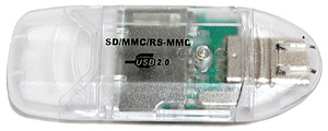
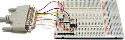
Sockets for regular SD cards seem to be relatively expensive for what they are, but the above SD card reader cost a pound (what else?) from Poundland. A bit of work with a soldering iron and some desoldering tools yielded some useful components:
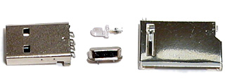
The crystal is unmarked and I'm hardly short of LEDs but the USB A connector could be a good way to reduce the size of a project that plugs into a USB port (USB B connectors are rather bulky) and the SD card slot works brilliantly for my needs here. There are cheaper and nastier ways to add an SD card slot to your project, but something like this feels more robust and has the advantage of reporting the state of the card's write protection switch.
Keyboard input and RAM disks make CP/M more useful
Wednesday, 16th June 2010
The hardware for the computer has changed in (mostly) subtle ways since the last post, with the exception of a PS/2 socket for connection to a keyboard.
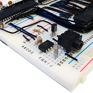
PS/2 keyboards (which use the same protocol as the older AT keyboard) communicate with the host by clocking data in either direction (keyboard to host or host to keyboard) over two wires, appropriately named "clock" and "data". An AVR pin change interrupt is used to detect a change in state of the clock line and either input or output a bit on the data line depending on the current direction of data transmission. Incoming bytes generally relate to the scancode of the key that has just been pressed or released. These scancodes are looked up on a series of hard-coded tables to translate them into their corresponding ASCII characters. CP/M accesses the keyboard via two BIOS routines: CONST (2), which checks whether a character is available or not, and CONIN (3), which retrieves the character. I initially implemented these by simply reading from I/O port 2 (CONST) or port 3 (CONIN).
As keyboard input is polled, CP/M was wasting a lot of time reading from the AVR. Due to the AVR's relatively slow way to respond to I/O requests this was slowing down any program that needed to periodically call CONST (for example, BBC BASIC constantly checks for the Escape key when interpreting BASIC programs). I converted this polling system into an event driven one by connecting the AVR to the Z80's maskable interrupt pin, /INT. When a new key is received by the AVR it pulls /INT low to assert it. The Z80 responds to the interrupt request by setting an internal flag to remember that a key has been pressed and acknowledges the interrupt by outputting a value to port $38 (the Z80's maskable interrupt handler resides at a fixed address of $38 in memory, so this seemed like a sensible choice). The AVR detects this write to port $38 and returns /INT to its high state. The CONST routine can now directly return the value of this flag when polled (rather than having to request the flag from the AVR) which noticeably speeds up running programs. The flag is cleared when a key is read by calling CONIN.
I did have some difficulty getting the interrupt system to work; the Z80 has a number of different ways of responding to interrupts, two of which rely on fetching a value from the data bus by asserting /IORQ before an interrupt is serviced. IM 0 fetches an instruction from the bus and executes it, and IM 2 fetches the least significant byte of the address of the interrupt service routine to combine with the most significant byte stored in the I register. IM 1 (which is what I'm using) just jumps to the fixed address $38. However, I hadn't taken this additional data read into account and when the Z80 attempted to read from an I/O device the AVR was either putting nonsense on the bus or (deliberately) locking up with a message to indicate an unsupported operation. Fortunately you can easily tell the difference between a regular I/O request and an interrupt data request by checking the Z80's /M1 output pin, so with that addition things started working a bit more smoothly!
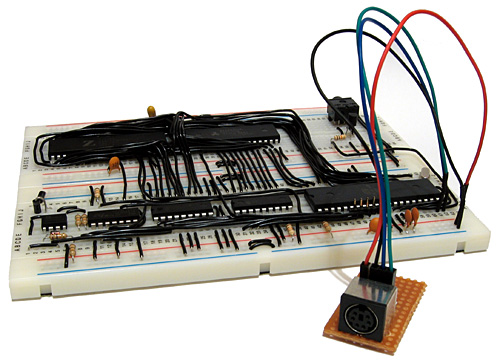
I'm still using terminal emulation software on my PC to view the output of the computer, though as I now have keyboard entry the results are a little more impressive than the few boot report lines and a prompt that were in the last entry. I still haven't worked out why my PC switches off or blue-screens when programming AVRs over the serial port, so I've soldered together a parallel port programmer for the time being.
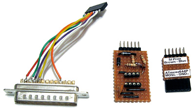
The pinout of the programmer matches that of the website where I found the SI Prog design. The ATmega644P's SPI, power and reset pins that the programmer interfaces with are all adjacent, but not in the same order as the ones in the SI Prog, hence the small board to the right of the above photo which swaps the pin order around using wires soldered to its reverse (this saves a lot of breadboard space). The board in the middle plugs directly into the parallel port programmer and is used to program the 512KB flash memory chip I'm using for storage.
I haven't got around to implementing writing to this flash memory yet, unfortunately, though I have implemented a simple way to test a writable disk drive. The RAM chip I am using is a 128KB one, as Farnell didn't sell 64KB ones. The Z80 can only address 64KB without additional memory banking hardware, so I'd simply tied A16 low and was ignoring half of the memory. I have now edited the BIOS to expose two disk drives; the default A: (512KB of flash memory) and now B:, a 64KB RAM drive. A16 is now driven by the AVR; during normal operation, it is held low (giving the Z80 access to its usual 64KB) but during disk operations it can be driven high to grant the AVR access to the previously hidden storage.
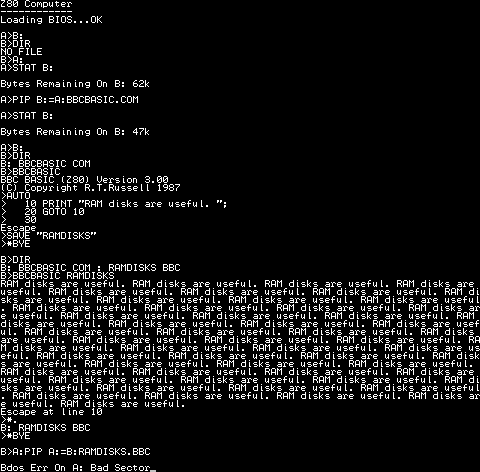
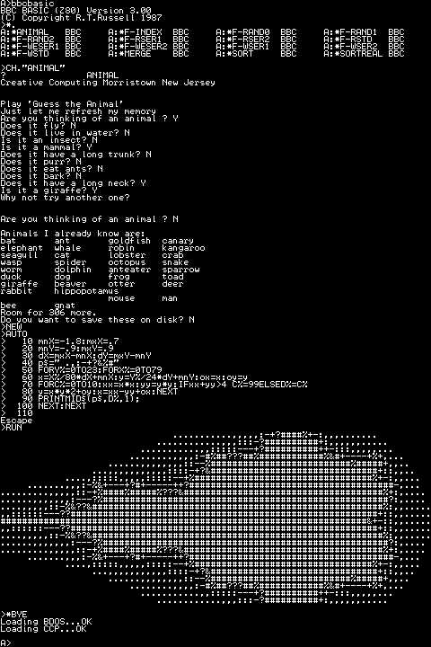
In the above test I use the STAT command to check free space, the PIP command to copy BBCBASIC.COM from A: (flash) to B: (RAM) then run BBC BASIC from the RAM disk, save a program then run it again by passing its filename as a command-line argument to BBC BASIC. At the end I try to copy the new program back to A:, but as there is no writing support for flash it keels over with a fairly unhelpful generic CP/M error.
Now that I've finally got something working in a vaguely usable manner, I hope I can start to research ways to make it better. Sorting out writing to flash would be a good start (I'm sorely tempted by jbb's suggestion to use an EEPROM to map logical floppy sectors to physical flash sectors) and I certainly hope to dig out my 320×240 pixel graphical LCD and driver for output instead of relying on a desktop PC. I'd also like to upgrade to CP/M 3 (I'm currently using CP/M 2.2) but when I last looked at that it seemed like a much more involved process so I decided to keep it simple. There's a fair mountain of stuff I need to take in, but I'm certainly learning a lot as I go (I only just realised tonight that CP/M was capable of graphics output, for one). I'd be a very happy chap if I could eventually run WordStar on this computer!
Combining a Z80 and an ATmega644P to boot CP/M
Monday, 14th June 2010
I've been working on a new Z80 computer over the last few days. I would say that I had been working on the existing Z80 computer were it not for the fact that this a completely new design.
The previous computer had two 32KB RAM chips to provide a total of 64KB RAM. To run a user program you need to get it into RAM somehow, so I also included a 128KB ROM chip which occupied the lower 16KB of the Z80's address space to provide the fixed operating system that could be used to load programs. By adding memory banking hardware I could select one of eight 16KB pages of ROM. The next 16KB was one of two banks of RAM from one RAM chip, and the final 32KB was mapped directly to the other RAM chip.
This is all fairly complicated, and not very flexible. Programs written for CP/M tend to be loaded into memory starting at address $0100, which is impossible with my old design as that section of memory is taken up by ROM.
Giving another device access to the buses
The Z80 accesses memory and other hardware devices using three buses; an eight-bit data bus which shuttles bytes of data between the various chips, a sixteen-bit address bus which addresses a location in memory or a particular I/O device, and a control bus which contains numerous lines that specify the type of operation (for example, if /MREQ and /WR go low together it indicates that a byte is being written to memory, or if /IORQ and /RD go low together it indicates that a byte is being read from an I/O device).
There is also a pin named /BUSREQ that can be used to request access to these buses. The Z80 will periodically check this pin and if it is held low it will put the data, address and control buses into a high-impedance state and drive /BUSACK low to acknowledge this. This effectively removes the Z80 from the circuit, and another device can now drive the buses.
;if(img.style.backgroundImage){img.style.backgroundImage='url('+img.src+')';img.src=imgs[img.src.indexOf(imgs[1])<0?1:2]}else{img.style.backgroundImage='url('+img.src+')';img.src=imgs[2];};void(0);)
This is the feature which I have based the new design around — the current prototype is pictured above. It features a Z80 and 128KB of SRAM (only 64KB is currently addressable) on the upper board. On the lower board is an ATmega644P microcontroller, which is used to start the computer.
When the circuit is reset, the ATmega644P requests access to the buses from the Z80. When access has been granted, it proceeds to copy the CP/M BIOS from the 512KB flash memory IC to a specific location in RAM (currently $F200). It then writes the Z80 jump instruction jp $F200 to the start of memory, returns control of the buses to the Z80 and pulses its /RESET pin. The CP/M BIOS then runs directly on the Z80.
As the ATmega644P doesn't have enough pins to drive all of the buses directly, I've added sixteen GPIO pins by using two MCP23S08 8-bit I/O expander chips. These are used to drive or sample the Z80 address bus; the data and control buses are driven or sampled directly by the GPIO ports on the ATmega644P.
Using a slow to respond microcontroller for I/O
The Z80 is most useful if it can talk to the outside world somehow, which is usually achieved by reading from or writing to I/O devices. In my previous design I built these out of latches and lots of glue logic. As I've added a powerful microcontroller to the computer which features a number of useful on-board peripherals, it would seem sensible to use that instead.
One problem with this idea is that the Z80 expects to read or write to an I/O device in a mere four clock cycles. The AVR has a delay between an interrupt occurring (such as a pin state changing) and executing interrupt service routine of at least five clock cycles. Even though the AVR is running at twice the clock speed of the Z80 this still doesn't provide much time to sample the address bus and perform some useful action before returning a value to the Z80. Fortunately, the Z80 has another useful pin, /WAIT, specifically to address this concern. By pulling this pin low the Z80 can be stalled, allowing the I/O device plenty of time to respond. I have included a 7474 D-type flip-flop as an SR latch to control the /WAIT pin. When the Z80's /IORQ pin goes low the flip-flop is reset, which pulls the /WAIT pin low. When the AVR notices that the /IORQ line has gone low it samples the address bus, performs the requisite task then sets the flip-flop, which drives the /WAIT pin high again and the Z80 continues executing the program.
The 7474 is a dual D-type flip-flop, so I have used the second flip-flop to halve the AVR's 20MHz clock signal to provide the 10MHz clock for the Z80.
CP/M interacts with the host computer by calling numbered BIOS functions. I have implemented a number of these BIOS functions by outputting a value to a port number that matches the BIOS function number. For example, CONOUT is function number four and is used to send the character in register C to the console.
CONOUT:
    ld a,c
    out (4),a
    ret
The AVR detects a write to port 4 and sends the incoming byte to one of its UARTs. I have connected this UART to a simple transistor inverter (pictured in the top right of the above photograph) and plugged the output from that into one of my PC's serial ports, so by running a terminal emulator I can see the output of CP/M on the screen. I have implemented only a handful of other functions (WBOOT outputs a value to port 1 to indicate that I should load the BDOS and CCP into RAM from the flash memory and READ can be used to copy 128 byte floppy disk sectors from flash memory to Z80 RAM) so the results are not exactly impressive:
Loading BIOS...OK
Loading BDOS...OK
Loading CCP...OK

A>
As I haven't implemented console input yet there's no way to type at the prompt, but that it gets that far is encouraging.
I haven't implemented writing to the flash memory due to a mistake I made when reading its datasheet. When writing to flash memory the value you write is ANDed with the data that's already there (you can only set a 1 bit to a 0 bit, but not vice-versa) – this is referred to as programming. If you want to write a 1 bit you have to erase the memory before writing to it (this is unsurprisingly referred to as erasing). Flash memory can be split into pages (small regions, in this case 256 bytes) and sectors (large regions, in this case 64KB). You can often program any number of bytes (up to a page at a time, aligned to page boundaries) but can only erase in larger blocks — pages, sectors, or the entire memory (bulk erase). I thought that the flash memory ICs I bought supported page erasing, but they only support sector erasing. CP/M transfers data between floppy disks and RAM in 128 byte floppy disk sectors, so to write an updated sector I would need to read 64KB from the flash memory, update a 128 byte region within it, erase an entire flash sector, then program the 64KB back to it. This would be very slow and quickly wear out the flash memory, so I am looking for some replacement flash memory ICs which do support page erase.
To copy the system files and a sample disk image to the flash memory I cobbled together the above parallel port programmer which is driven by an application cobbled together in C#. It's rather slow but gets the job done — unlike my AVR programmer. After finally managing to get CP/M to boot in a satisfactory manner I made a few tweaks to the AVR program and hit the "Build and Program" button in the editor. The code built, but rather than program the AVR my computer switched off. No error message, not even a blue screen, just a sudden and surprising power down. Since then I've only managed to talk to the AVR once; every other time has resulted in either a power down or blue screen. I had hoped to add some keyboard handling routines to the project to at least be able to interact with CP/M, but after fiddling around for an hour and a half without managing to get anything working again I gave up. I wish I knew why it suddenly stopped working, after hours of reliable service — maybe it's a hint that it's time to buy a proper USB debugger rather than the cheap and cheerful home-made serial port programmer I've been using!
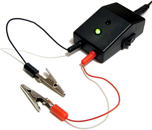
One equally cheap but useful addition to my tools is the above 5V power supply (yes, it's just a 7805 regulator in a box). Every project I have built needs a 5V supply from somewhere, which usually comes from a 7.5V wall wart power supply unit regulated to 5V with a 7805. This takes up valuable breadboard space and the weight of the cable from the power supply tends to drag the breadboard around the smooth surface of my desk, so having a dedicated box with an on-off switch, indicator LED, reverse voltage protection and an easy way to connect to the circuit via 2mm sockets is very handy indeed.
I now need to find a way to program AVRs without my PC switching itself off before I can make any more progress on the project...
ATmega644P CHIP-8/SCHIP interpreter
Sunday, 7th March 2010
In an attempt to solve the screen resolution problem issue I've bought a very cheap 320×240 pixel graphical LCD – a PG320240H-P9 on eBay for $24. Part of the reason for its cheapness may be down to its the lack of a controller; you need to constantly refresh the LCD with pixel data yourself (easier to use modules have integrated controllers that refresh the display for you from some on-board RAM). If I manage to get it working I'll have a 128×64 pixel graphical LCD going spare – finding a use for it could make an interesting project.
I have a bit of a soft spot for the CHIP-8 programming language, having previously written an few implementations. The CHIP-8 environment requires just under 3.5KB of RAM, and my recent investment in an ATmega644P boasting 4KB of RAM provided me with a microcontroller that was up to the task.
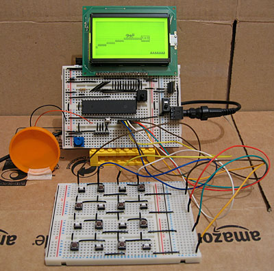
Beyond the ATmega644P and LCD the hardware is pretty simple; a potentiometer is provided to adjust the speed of the interpreter when it's running, from 1/8th speed up to 8× speed. Sound is output using a piezo transducer, which I've taped to the hard plastic lid from a tube of chocolates to amplify it. Games rely on a 4×4 hex keypad for input, and as I do not have a 4×4 keypad – hex or otherwise – I assembled my own on another breadboard. I don't even have sixteen switches of the same type, hence the mixture in the above photo. A schematic of the hardware can be downloaded in PDF format.
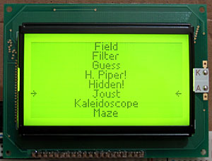
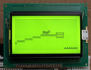
When you reset the circuit a list of all of the programs stored on the microcontroller is shown on the LCD. The 64KB of flash memory on the ATmega644P is enough to store the code for the interpreter and all of the CHIP-8 and SCHIP games available on the Internet. For a change I've decided to have a go at designing a variable width font rather than use one of my existing fixed-width fonts; I don't think it looks too shabby.
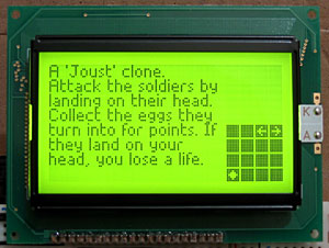
When a game has been selected a (gramatically incorrect) summary of the game is shown. To the right of the screen is a 4×4 grid informing the player which key does what; arrows for directional controls, a diamond for "fire" or confirmation actions and a tick/cross for yes/no input. There doesn't seem to be any particular convention for keypad input in CHIP-8/SCHIP games, which makes this feature invaluable!
Subscribe to an RSS feed that only contains items with the ATmega644P tag.