dsPIC33 VDC with GLCD or PAL TV output
Sunday, 4th July 2010
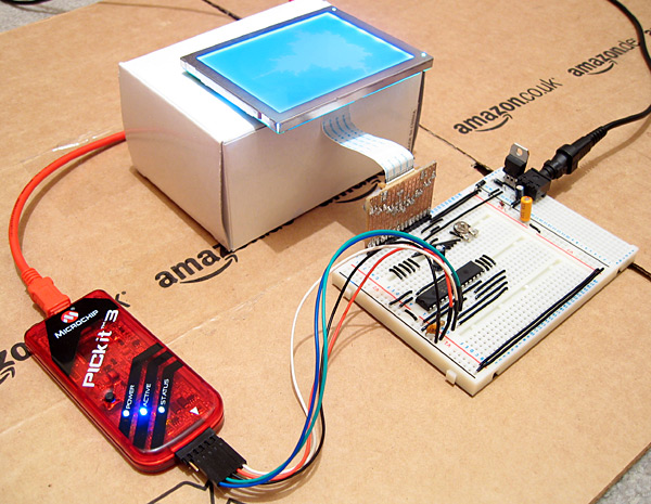
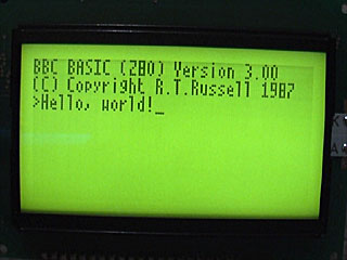
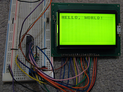
I have currently been using some terminal emulation software on my PC to see the output of the Z80 computer. It seems a little silly to rely on a large multi-gigahertz, multi-megabyte machine just to display the output from a machine at the megahertz and kilobyte end of the scale. I had previously done some work with a dsPIC33 to drive a 320×240 pixel graphical LCD so dug out its breadboard and dusted off the code to try to make something of it.
Inspired by John Burton's recent experiments with PAL TV output I decided that the first thing I should do is add support for TV output. The graphical LCD is nice but a little small and responds to pixel changes rather slowly, making animation very blurry.
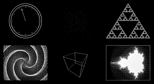
I think the results are reasonably good. A lot of the code is shared with the old LCD driving code, which means that the LCD demos work fine with the TV too. Fortunately, retracing the TV is a much less CPU-intensive job than retracing the LCD. The PIC has an SPI peripheral that allows you to clock out eight or sixteen bits a bit at a time at a selected speed by writing to a single register, which is great for clocking out the pixel data on each scanline. Even better are the PIC's DMA channels, which allow you to output a selected number of bytes or words to a selected peripheral from a specified location in RAM with no CPU involvement; all I need to do on each line is to copy a complete scanline to the DMA memory, initiate a transfer from this memory to the SPI peripheral and the job is as good as done. Using the DMA hardware as opposed to writing to the SPI registers directly reduced the rendering time of the Mandelbrot fractal part of the demo from 33 seconds to 18 seconds.
One problem I haven't been able to resolve is that the PIC inserts a small delay between every DMA/SPI transfer, which results in every sixteenth pixel being a bit wider than the fifteen before it. This is especially noticed on dithered regions. If I write to the SPI registers directly this delay vanishes. I'm not sure if the picture quality increase is worth the loss of performance, so I'd rather find a proper fix for this! For the time being, here's a video of the demo as it currently runs:
The TV contains a 75Ω resistor to ground on its composite video input. Two resistors are used on two PIC pins to form a voltage divider to produce the required output voltages (0V for sync, 0.3V for black and 1V for white). When the TV is disconnected the output of the circuit is 3.3V (the supply voltage, equivalent to a logic "high") as there's no load resistance to pull it to the correct 0.3V (a logic "low"). This can be used to periodically check whether a TV is connected and to switch between the LCD and TV output modes.
The above is rather vague, and I would recommend Rickard Gunée's article entitled How to generate video signals in software using PIC for more detailed information! The code for the demo can be downloaded from my website for those who are interested.
Update: I've updated my code to use the SPI peripheral in slave mode and use a timer and output compare unit to generate the clock signal. This regular clock signal produces pixels of identical sizes the new code can be downloaded here.
Controlling a PG320240H-P9 with a dsPIC33FJ128GP802
Sunday, 21st March 2010
In a previous entry I mentioned that I had purchased a PG320240H-P9 graphical LCD. This is a 320×240 white-on-blue pixel display, and it does not have an on-board controller or RAM. To display something on it you need to constantly refresh it with picture data; in this instance, sending four pixels at a time, starting from the top left and working from left to right, top to bottom — a bit like the scanning pattern of a CRT monitor.
Connecting a circuit to the LCD is made slightly more tricky by its use of a 16-pin 1mm flexible flat cable. To get around this I soldered together an adaptor using a suitable FCC connector, pin strip, piece of stripboard and a fairly excessive quantity of hot melt adhesive. Even more tricky was the lack of a suitable datasheet for the LCD. After some digging I located this one for the PG320240WRM-HNNIS1 — it's slightly different, but contains timing diagrams and specifications that seem to work with the LCD I bought. One thing I still haven't worked out is the contrast adjustment; a 5K variable resistor between 0V and the relevant pin seems to have had the best results thus far. A helpful webpage, Graphical LCD controller for ST8024+ST8016 based displays, has a plain English description of how to drive the LCD, though as far as I'm aware the M pin should have its logic level toggled every frame, giving you a "glass" frequency of half of the refresh rate, not 200Hz-400Hz. The lack of a proper datasheet makes these things a little complicated!
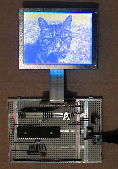
My first attempt to drive the LCD involved an ATmega644P, a microcontroller with 64KB of flash ROM and 4KB of RAM. The above photo shows it displaying a picture of a cat, which was stored in ROM and output using the following code:
#include <stdint.h>
#include <avr/io.h>
#include <avr/pgmspace.h>

#define LCD_FLM   (6)
#define LCD_M     (5)
#define LCD_C1    (4)
#define LCD_C2    (3)
#define LCD_D_OFF (2)

#define LCD_CONTROL_PORT (PORTC)
#define LCD_CONTROL_PIN  (PINC)
#define LCD_CONTROL_DDR  (DDRC)

#define LCD_DATA_PORT    (PORTA)
#define LCD_DATA_PIN     (PINA)
#define LCD_DATA_DDR     (DDRA)

#include "cat.h"

int main(void) {

    // Make control pins outputs.
    LCD_CONTROL_DDR |= _BV(LCD_FLM) | _BV(LCD_M) | _BV(LCD_C1) | _BV(LCD_C2) | _BV(LCD_D_OFF);

    // Make data pins outputs.
    LCD_DATA_DDR |= 0b1111;

    // Enable the LCD.
    LCD_CONTROL_PORT |= _BV(LCD_D_OFF);

    for(;;) {

        // Toggle the M pin to provide the LCD AC voltage.
        LCD_CONTROL_PIN |= _BV(LCD_M);

        const uint8_t* picture_ptr = cat_picture;

        // Scan 240 rows in the image.
        for (uint8_t row = 0; row < 240; ++row) {

            // Begin the line.
            LCD_CONTROL_PIN |= _BV(LCD_C1);
            LCD_CONTROL_PIN |= _BV(LCD_C1);

            if (row < 2) LCD_CONTROL_PIN |= _BV(LCD_FLM);

            // Send 40 eight-bit words.
            for (uint8_t column = 0; column < 40; ++column) {
                LCD_DATA_PORT = pgm_read_byte(picture_ptr) >> 4;
                LCD_CONTROL_PIN |= _BV(LCD_C2);
                LCD_CONTROL_PIN |= _BV(LCD_C2);
                LCD_DATA_PORT = pgm_read_byte(picture_ptr);
                LCD_CONTROL_PIN |= _BV(LCD_C2);
                LCD_CONTROL_PIN |= _BV(LCD_C2);
                ++picture_ptr;
            }
        }
    }

}
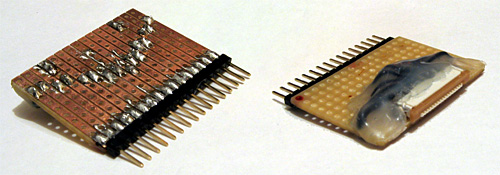
A 320×240 display has 76,800 pixels, and if you store each pixel as a single bit (so eight pixels per byte) you need 9600 bytes to store a complete frame, which clearly won't fit in the 4KB offered by the ATmega644P. Rather than upgrade to an AVR with more memory, I jumped to the dsPIC33FJ128GP802, a 16-bit microcontroller with 16KB of RAM. As well as quadrupling the RAM from the ATmega644P it also doubles the program memory (128KB from 64KB) and speed (40 MIPS from 20 MIPS). When working with AVRs I'd been using a slow home-made serial programmer, and rather than continue with this sorry state of affairs (lack of debugging capabilities is never fun, especially when it takes over a minute to program the microcontroller) I treated myself to a PICkit 3 Debug Express.
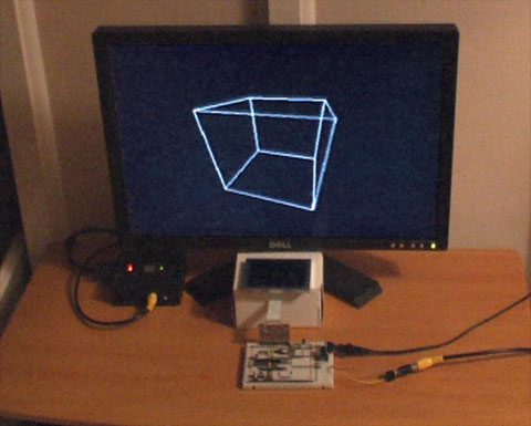
The above photo shows the LCD connected to the microcontroller as well as the PICkit 3. The dsPIC33FJ128GP802 requires a voltage supply from 3.0V to 3.6V, not the 5V I am used to, so to power it I have put two IN4001 rectifier diodes in series with the 5V regulator output. Each diode incurs a voltage drop of 0.7V, producing 3.6V for the rest of the circuit. The LCD is powered from the main 5V supply, but it seems happy with the 3.6V logic "high" from the dsPIC.
The LCD is connected to the dsPIC as follows:
- FLM to RB15
- M to RB14
- C1 to RB13
- C2 to RB12
- /D_OFF to RB11
- D0~D3 to RA0~RA3
A 10K resistor is included between /D_OFF and ground. This is very important, as it holds the /D_OFF line low when RB11 is floating (e.g. during reset), forcing the display off — if the display is powered, but is not being actively refreshed, the LCD panel can become overloaded and damaged.
I have knocked together a simple demo that shows a few different graphics on the LCD. The LCD is constantly refreshed by an interrupt service routine that runs in the background, leaving some CPU time to the user program. As there is only enough RAM for a single frame buffer, animation has to be quite simple to avoid flickering, but I've still managed to include my favourite spinning cube.
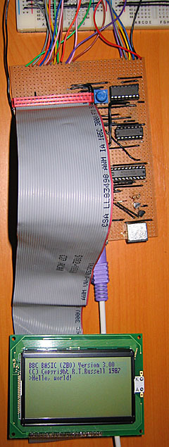
The project can be downloaded here. I'm still getting to grips with the dsPIC series; the code is likely to be pretty awful, and I still have a problem where the dsPIC resets itself every couple of minutes (I'm not really sure if this is a software or hardware issue). Still, it's a start, and I hope that I can use this LCD as the display for my Z80 computer project.
Update: Having seen this post, the chap who originally suggested that I investigate the dsPIC33FJ128GP802 sent me an email with some advice, chiefly about my poor power supply, missing decoupling capacitors and use of an electrolytic capacitor on the VCAP pin. I have since replaced the two rectifier diode affair with a proper 3.3V regulator for the power supply, added a decoupling capacitor across AVDD/AVSS and moved the decoupling capacitor between VDD/VSS closer to the microcontroller. I have also ordered some tantalum capacitors to replace the electrolytic one. A bit of debugging found that the watchdog timer is responsible for the spurious resets; I have disabled it in the code for the time being, which has stopped the resets.
2MHz should be enough for anyone
Wednesday, 27th August 2008
 LCD Timing
Last time I discussed the hardware I mentioned I had LCD timing issues. I have finally resolved them, but this has been the most time consuming part of the project so far.
The first thing to sort out was the LCD's E pin. Once you have set up the LCD's input pins to a state where they're ready to read or write data, you need to drive this pin high. I had had some success by holding it high permanently and relying on the Z80 to set all the other to the right state at roughly the same moment, but this was inaccurate and resulted in occasional display glitching.
Consulting the datasheet, it appears that once the input pins are ready E needs to be held low for at least 450nS and then needs to be driven high for at least 450nS. Hmm. During an I/O request (and once the Z80 has prepared the address and data bus) there's a delay of 1 clock cycle, then /IORQ is held low for about 2.5 CPU cycles. That is the window of opportunity. I have connected a binary counter to the Z80's clock signal and take the least significant bit of the output - every clock cycle this output toggles between a low and a low, effectively halving the CPU clock rate. I then connect the counter's reset pin (which overrides the clock input and forces it to output zero) to /IORQ. The result is that when the Z80 is not accessing hardware the counter is held in its reset state, and E is held low. When the Z80 holds /IORQ low, the counter starts up and outputs a zero for one CPU cycle, outputs a one for the next CPU cycle, then outputs a zero for the next half clock cycle at which point /IORQ goes high again and it is back to zero anyway. This is exactly what's needed!
This also allows us to calculate the maximum CPU clock rate. If we are generous and allow E to be low for 500nS then high for 500nS, that gives us a CPU clock rate of 1/500nS=2MHz.
Anyhow, that's one problem resolved, but there was still one nasty bug. When reading from the LCD it would occasionally end up writing to the area that was being read or, in worse cases, the Z80 would "crash". The LCD has a R/#W pin that is held high when reading and held low when writing. I had connected it directly to the Z80's /WR pin, which is high normally and low when writing. The problem here is "normally" as the LCD was expecting to be read even when the Z80 wasn't requesting a /RD. When being read, the LCD expects to put something onto the data bus, and it appeared that it kept thinking that it needed to put something on the bus when it wasn't needed. This caused fighting with the other chips that were trying to put their own values on the data bus, hence the crashes as the Z80 received invalid data.
The answer was very easy; simply connect the Z80's /RD pin to the LCD's R/#W pin via a NOT gate. In the default state the pin is held low (LCD expects a write and leaves the data bus alone), and only goes high during a /RD. The LCD interface is now very robust.
CPU Clock
Above I mention the calculation for the maximum clock rate. Rather than use the 555 for timing, I switched to using a 10MHz crystal resonator oscillator. I'm using the serial resonant circuit from z80.info with a 74F04 hex inverter (second circuit down). Fortunately the counter chips I have are decade counters (ie, designed to count from 0 to 9) made up of a ÷2 and a ÷5 section. I can connect a 10MHz oscillator to the ÷5 section and use the output of that to drive the CPU. In the final design I'd like to add a "hardware control port" with a bit that would let the programmer choose 2MHz or 10MHz mode by setting or resetting a particular output bit (other control bits would include switching the LCD backlight on or off and a buzzer for beeping sound output).
PS/2 Ports
As a friend pointed out, the 8-bit open-collector I/O port (which will drive two PS/2 ports, the I2C bus and TI calculator link port) had a flaw - there was no resistor on the base of the output transistors. The result is that if the output latch tries to drive the transistor base high, the transistor switches on and shorts the output of the latch to ground. This was clearly a problem in the design as the LCD backlight dimmed when trying to output to these ports as they drew a excessive amount of current when effectively short-circuited. A 22K resistor between the output latch and base of the transistor fixed the problem.
In the above photo, I've also added two 100K resistors to hold the output high when floating, but only to the foreground PS/2 port for the time being. I don't think I'll be controlling a mouse yet!
Revised OS
With a little modification of the Emerson PS/2 library I've got a basic keyboard driver up and running on the hardware. All the OS does for the moment is check for keys and display them on the screen. It's currently hard-coded to the UK layout, as I haven't yet decided how I'm going to handle storage and by keeping the layout in ROM it at least frees up a few hundred bytes of RAM that would otherwise need to be there for the scancode translation tables.
Z80 computer with a primitive I/O board
Wednesday, 20th August 2008
A computer needs some way of interacting with the outside world via input and output devices. It's about time, then, that the Z80 computer project acquires a section dedicated to I/O.
The Z80 differentiates between memory and I/O devices, though both share the data bus and the address bus. You can control I/O devices using the in (input) and out (output) instructions. When you input or output you must specify a device address and a value or target register. For example,
    in a,($20) ; Read a value from device $20 and store it in A.
    ld a,123
    out ($40),a ; Output 123 to device $40.
When you write to a device, the following happens:
- The address bus is set to the address of the device to output to.
- The data bus is set to the value to be written to the device.
- The /IORQ and /WR pins on the Z80 go low.
- The device processes the written data.
- The /IORQ and /WR pins on the Z80 go high.
Reading from the device is very similar:
- The address bus is set to the address of the device to read from.
- The /IORQ and /RD pins on the Z80 go low.
- The device puts the value to read onto the data bus.
- The Z80 reads the value on the data bus.
- The /IORQ and /RD pins on the Z80 go high.
(Accessing memory is a similar procedure, except with the /IORQ pin replaced by the /MREQ pin).
Interfacing I/O devices to a Z80 CPU should be rather straightforwards, then. I am using a 74HCT138N 3-to-8 line inverting decoder to handle the address bus input and /IORQ signal. This IC has three address inputs and 8 outputs. If the address input is %000, output 0 is low and all the other pins are high; if the address input is %001 output 1 is low and all the others are high; if the input is %010 output 2 is low and all the others are high (and so on and so forth). /IORQ is connected to another input on the chip, /E1, which causes all of the pins to go high when it is high regardless of the address input.
What does this mean in practice? Well, most devices have a "chip enable" or "chip select" input pin. When this input is active the device performs its function, but when the input is not active the device is deactivated and doesn't respond to any other inputs or output anything. By connecting each output of the 3-to-8 decoder to a particular device's chip enable pin I can ensure that each device is only activated when its address is specified on the address bus and the /IORQ pin on the Z80 is low.
I have connected the Z80's A5-A7 to A0-A2 on the 3-to-8 decoder. This means that the first device has a base address of $00, the second $20, the third $40 and so on at increments of $20. This might sound a little odd, but has a reason. Some devices, such as the LCD, have sub-addresses of their own. In the case of the LCD, it has a pin that specifies whether you're dealing with an instruction (such as a command to switch the display on or off or read the LCD status) or some data (which forms part of the picture on the LCD). By attaching this pin directly to the Z80's A0 and the LCD's chip select pin to output 1 from 3-to-8 decoder you end up with an LCD instruction port at $20 and an LCD data port at $21.
An LCD is all well and good, but we'll need to take input from the user. To accomplish this, I'm going to supply two PS/2 ports and implement the AT protocol (as used by PS/2 keyboards and pointing devices) in software. Each device only requires two open-collector data lines (data and clock), so a single I/O device that provides eight I/O lines would be useful.
The design I'm going for uses two 74AC373 octal transparent latches. When the latch enable input pin is held high whatever value is on the input passes through to the corresponding output. When the latch enable pin goes low, the last value that was latched at the input is still output. These particular latches also have an output enable pin that can be used to disable the outputs and let them "float" (ie, other devices can then drive that particular connection high or low as required). In this instance, one latch has its output enable pin activated so that it always outputs the last value written to it and has its latch enable pin connected to the Z80's /WR pin. The other latch has its latch enable pin activated so that it always outputs the values at its input and has its output enable pin connected to the Z80's /RD pin.
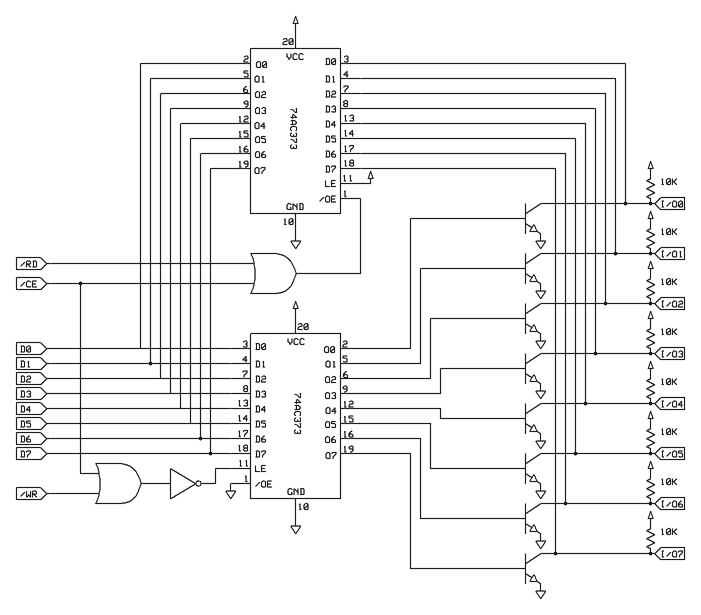
The transistors on each output are used to provide open-collector outputs. When the base of the transistor is held low, the transistor is "switched off" and its output floats, and so can be driven by external circuitry. When the base of the transistor is held high, it switches on and effectively connects the output to ground. A pull-up resistor ensures that the pin has a high signal when not connected to anything. This arrangement is useful as each pin can be driven low by either device and so works as an input or an output (for a real-world example, an AT keyboard usually outputs a clock signal on one line to the host when sending data, but if the host pulls the clock line low it can inhibit communication and the keyboard buffers the data to send instead).
;if(img.style.backgroundImage){img.style.backgroundImage='url('+img.src+')';img.src=imgs[img.src.indexOf(imgs[1])<0?1:2]}else{img.style.backgroundImage='url('+img.src+')';img.src=imgs[2];};void(0);)
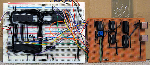
Rather than build the circuit on breadboard, I went straight to stripboard. The above photo shows an incomplete version of the output board. Only one PS/2 port is wired up at all! The pin header to the left is to connect the LCD to. The coloured wires at the extreme left connect this I/O board to the rest of the computer.
;if(img.style.backgroundImage){img.style.backgroundImage='url('+img.src+')';img.src=imgs[img.src.indexOf(imgs[1])<0?1:2]}else{img.style.backgroundImage='url('+img.src+')';img.src=imgs[2];};void(0);)
I have modified the Z80 board I was using last time to add support for RAM. The 3-to-8 decoder in the bottom right is used to partition the address space into two 32KB regions. The lower 32KB is mapped to ROM, and the upper 32KB is mapped to RAM. This wastes 75% of the ROM chip (it's a 128KB chip) but without a more complex memory management unit this will have to do for the moment. The most significant bit of the address bus, A15, is fed into the 3-to-8 decoder along with the /MREQ pin.
The test software is a Z80 program that displays an animation on the LCD using 20 frames (1KB per frame) stored in ROM.
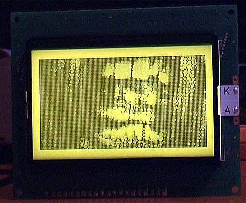
The Z80 is still not breaking MHz speeds, but there are problems here. I have not interfaced the LCD correctly, as its timing patterns for reading and writing data are quite different to those used by the Z80. Bizarrely, holding the E pin on the LCD permanently high appears to work 99% of the time, even though the datasheet indicates that it should be used to clock data in or out. The result is glitches in the data sent to the LCD, usually on the left hand side (the left hand side of the display has a propensity to believe it's been sent the "switch off" command). I'm not sure I'll be able to remedy this situation. Judging by the datasheet it looks like the LCD does its stuff when the E pin goes from a low to high state (the Z80 does everything when /IORQ goes low), so maybe simply inverting /IORQ and pumping it into E will do the trick.
Back to Hardware
Friday, 1st August 2008
I enjoy dabbling with low-level programming, but have never actually built a computer to run these programs. I think it's time to correct that, and as the BBC BASIC project has required me to develop an almost complete Z80 OS (the only thing that's left for the TI-OS to do is manage files) I thought a Z80 computer would be a good start.
The planned specs are (as a starting point):
- 10 MHz Z80180 CPU;
- 64KB RAM (2 32K×8 SRAM chips);
- 128KB Flash ROM;
- Graphical LCD;
- Simple joypad input;
- Keyboard input (AT using either software AT routines or dedicated microcontroller).
The first spanner in the works is the Z80180, as I didn't read the datasheet closely enough and it's in a DIP 64 package with 0.07" pin spacing instead of the standard 0.1" pin spacing. I'll need to find some way of constructing an adapter so I can use it with my breadboards and stripboard. 
In the meantime, I've concentrated on the graphical LCD. I picked a 128×64 backlit graphical LCD for the princely sum of £16. It's very easy to control - you hook up it up to a 8-bit data bus to transfer image data and instructions and a handful of control pins to indicate what you're doing on that bus (reading or writing, whether you're sending an instruction or some image data, that sort of thing) and that's it - the only supporting circuitry it requires is a 10K potentiometer to act as a contrast control and power for the display and backlight.
To experiment with the LCD, I'm using a PICAXE-28X1 microcontroller, programmed in BASIC. There isn't much space to store graphics, so I'm using a 32 character font (at eight bytes per character, that takes up all 256 bytes of free EEPROM space!)
; LCD data bus should be connected to port C.

Symbol LcdRegisterSelection = 0 ; D/I  :  4
Symbol LcdReadWrite         = 1 ; R/W  :  5
Symbol LcdStartEnable       = 2 ; E    :  6
Symbol LcdChipSelect1       = 3 ; CS1  : 15
Symbol LcdChipSelect2       = 4 ; CS2  : 16
Symbol LcdReset             = 5 ; /RST : 17

; Storage for console state variables.

Symbol ConsoleX             = B10
Symbol ConsoleY             = B11
Symbol ConsoleChar          = B12


	GoSub LcdInit                              ; Initialise LCD.
	B0 = %00111111 : GoSub LcdWriteInstruction ; Switch LCD on.

	GoSub LcdClear ; Clear LCD

	; Write the obligatory message to the LCD.

	ConsoleX = 0 : ConsoleY = 0

	ConsoleChar = $08 : GoSub LcdPutChar ; H
	ConsoleChar = $05 : GoSub LcdPutChar ; E
	ConsoleChar = $0C : GoSub LcdPutChar ; L
	ConsoleChar = $0C : GoSub LcdPutChar ; L
	ConsoleChar = $0F : GoSub LcdPutChar ; O
	ConsoleChar = $1D : GoSub LcdPutChar ; ,
	ConsoleChar = $00 : GoSub LcdPutChar ;
	ConsoleChar = $17 : GoSub LcdPutChar ; W
	ConsoleChar = $0F : GoSub LcdPutChar ; O
	ConsoleChar = $12 : GoSub LcdPutChar ; R
	ConsoleChar = $0C : GoSub LcdPutChar ; L
	ConsoleChar = $04 : GoSub LcdPutChar ; D
	ConsoleChar = $1B : GoSub LcdPutChar ; !

	Pause 2000

	B2 = 0
MainLoop:
	B2 = B2 - 1
	B0 = B2
	GoSub LcdGotoZ
	Pause 30
	GoTo MainLoop

LcdInit:
	DirsC = $00               ; Set data bus to input.
	High LcdStartEnable       ; We're not writing anything.
	High LcdChipSelect1
	High LcdChipSelect2
	Low LcdReset
	Pause 500
	High LcdReset
	Pause 500
	Return

LcdWriteInstruction:
	Low LcdReadWrite
	DirsC = $FF               ; Data bus = output.
	PinsC = B0                ; Set data bus state.
	Low LcdRegisterSelection  ; Instruction, not data.
	Low LcdStartEnable
	High LcdStartEnable
	DirsC = $00               ; Leave data bus floating.
	Return

LcdWriteData:
	Low LcdReadWrite
	DirsC = $FF               ; Data bus = output.
	PinsC = B0                ; Set data bus state.
	High LcdRegisterSelection ; Data, not instruction.
	Low LcdStartEnable
	High LcdStartEnable
	DirsC = $00               ; Leave data bus floating.
	Return

LcdGotoX:
	B0 = B0 And 7
	B0 = B0 + %10111000
	GoTo LcdWriteInstruction

LcdGotoY:
	B0 = B0 And 63
	B0 = B0 + %01000000
	GoTo LcdWriteInstruction

LcdGotoZ:
	B0 = B0 And 63
	B0 = B0 + %11000000
	GoTo LcdWriteInstruction

LcdClear:
	For B2 = 0 To 7
		B0 = B2
		GoSub LcdGotoX
		B0 = 0
		GoSub LcdGotoY
		B0 = 0
		For B3 = 0 To 63
			GoSub LcdWriteData
		Next
	Next B2
	Return

LcdPutMap:
	B1 = B0 * 8
	For B2 = 0 To 7
		Read B1, B0
		GoSub LcdWriteData
		B1 = B1 + 1
	Next B2
	Return

LcdPutChar:
	B0 = ConsoleY
	GoSub LcdGotoX
	B0 = ConsoleX * 8
	If B0 < 64 Then
		Low LcdChipSelect2
	Else
		Low LcdChipSelect1
		B0 = B0 - 64
	EndIf
	GoSub LcdGotoY
	B0 = ConsoleChar
	GoSub LcdPutMap
	High LcdChipSelect1
	High LcdChipSelect2
	ConsoleX = ConsoleX + 1
	If ConsoleX = 16 Then
		ConsoleX = 0
		ConsoleY = ConsoleY + 1
		If ConsoleY = 8 Then
			ConsoleY = 0
		EndIf
	EndIf
	Return

; Font
EEPROM $00,($00,$00,$00,$00,$00,$00,$00,$00,$7E,$7F,$09,$09,$7F,$7E,$00,$00)
EEPROM $10,($7F,$7F,$49,$49,$7F,$36,$00,$00,$3E,$7F,$41,$41,$63,$22,$00,$00)
EEPROM $20,($7F,$7F,$41,$63,$3E,$1C,$00,$00,$7F,$7F,$49,$49,$49,$41,$00,$00)
EEPROM $30,($7F,$7F,$09,$09,$09,$01,$00,$00,$3E,$7F,$41,$49,$7B,$3A,$00,$00)
EEPROM $40,($7F,$7F,$08,$08,$7F,$7F,$00,$00,$41,$41,$7F,$7F,$41,$41,$00,$00)
EEPROM $50,($20,$61,$41,$7F,$3F,$01,$00,$00,$7F,$7F,$1C,$36,$63,$41,$00,$00)
EEPROM $60,($7F,$7F,$40,$40,$40,$40,$00,$00,$7F,$7F,$06,$1C,$06,$7F,$7F,$00)
EEPROM $70,($7F,$7F,$0C,$18,$7F,$7F,$00,$00,$3E,$7F,$41,$41,$7F,$3E,$00,$00)
EEPROM $80,($7F,$7F,$09,$09,$0F,$06,$00,$00,$3E,$7F,$41,$31,$6F,$5E,$00,$00)
EEPROM $90,($7F,$7F,$09,$19,$7F,$66,$00,$00,$26,$6F,$49,$49,$7B,$32,$00,$00)
EEPROM $A0,($01,$01,$7F,$7F,$01,$01,$00,$00,$3F,$7F,$40,$40,$7F,$3F,$00,$00)
EEPROM $B0,($1F,$3F,$60,$60,$3F,$1F,$00,$00,$7F,$7F,$30,$1C,$30,$7F,$7F,$00)
EEPROM $C0,($63,$77,$1C,$1C,$77,$63,$00,$00,$07,$0F,$78,$78,$0F,$07,$00,$00)
EEPROM $D0,($61,$71,$59,$4D,$47,$43,$00,$00,$00,$00,$5F,$5F,$00,$00,$00,$00)
EEPROM $E0,($02,$03,$59,$5D,$07,$02,$00,$00,$00,$80,$E0,$60,$00,$00,$00,$00)
EEPROM $F0,($00,$00,$60,$60,$00,$00,$00,$00,$07,$07,$00,$07,$07,$00,$00,$00)
The code isn't very robust - it doesn't check the state of the LCD's busy flag as I'm assuming that a 4MHz PIC running an interpreted BASIC is too slow to manage to write another byte to the LCD driver before it has finished processing the last one.
The font was generated from the following image (it's the BBC Micro font):
It's rotated through 90° as, unlike the LCD driver in the TI-83+, each byte written outputs 8 pixels vertically, with the least significant at the top. (On the TI-83+, each byte written outputs 8 pixels horizontally, with the most significant bit on the left). More interestingly, this graphical LCD is made up of two 64×64 regions next to eachother, and by controlling two chip select pins you can control whether each byte written updates the left side, the right side, neither or both. I'm entirely sure how I could use this, though, other than not-very-exciting tricks like clearing the LCD extra-fast.
Finally, here's a video of the LCD test in action. It's not very speedy, but will hopefully pick up some speed once I figure out how I'm going to use that Z80180 CPU.
Subscribe to an RSS feed that only contains items with the LCD tag.