Times, backlights and off-page calls
Sunday, 14th September 2008
Dates, times and backlights
I'm using a DS1307 real-time clock to provide the computer with real-time date and time functions. It's a great little chip - all it needs is power, two lines for I2C communications, a 32768Hz crystal between two pins and a back-up battery to keep it ticking when main power is removed and it's happy. That accounts for seven pins; the last remaining pin can be used as a one-bit output (you can set it to a high or low state in software) or it can be configured to output a square wave at 1Hz, ~4kHz, ~8kHz or ~32kHz.
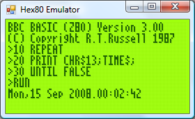
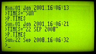
BBC BASIC can access the clock via the TIME$ pseudo-variable. This string variable returns the date and time in the format Sun,14 Sep 2008.15:20:00, and you can set the clock by assigning to the variable. When setting the clock you can specify either the date, the time, or both. Parsing the string has been an interesting exercise in Z80 programming, as it's not something I've ever attempted without regular expressions before!
The only hardware modification since last time is a very poorly implemented software control of the backlight. The fifth bit of the control port specifies whether the backlight is on or off, and it can be toggled with the *BACKLIGHT command. I say "poorly implemented" as the transistor driver I'm using to interface the hardware port with the backlight LEDs results in a much dimmer backlight than when I had the LEDs hooked up directly to the power supply (on the positive side, at least the 5V regulator's heatsink is cool enough to touch - the backlight draws a lot of current).
Calling off-page functions
Now that I have access to all eight 16KB "pages" that make up the 128KB OS ROM, it may help to explain how one can use all of this memory. After all, if page 1 is swapped in and you wish to call a function on page 2, a regular Z80 call isn't going to work as you need to swap page 2 before calling the function then swap page 1 back in afterwards.
The trick is to exploit the way that the Z80 handles calling subroutines. There is a 16-bit register, PC, which stores the address of the next instruction to execute. When you call a subroutine, the Z80 pushes PC onto the stack then sets PC to the address of the subroutine. When you return from a subroutine (via the ret instruction) the Z80 simply pops the value it previously pushed onto the stack and copies this back to PC. Instead of calling the target subroutine directly, you call a special handler that is available on every page. Following your call is 16-bit identifier for the off-page function you wish to call. This handler then (prematurely) pops off the return address from the stack, reads the 16-bit value that follows it (which is the indentifier of the function you wish to call), looks up the page and address of the target function, swaps in the correct page and calls it as normal. When the function returns, the handler then swaps back the calling page and jumps back to the return address.
The Z80 has a series of rst instructions that call fixed addresses within the first 256 bytes of memory. These instructions are useful as they're small (one byte vs three bytes for a regular call) and fast, so I'm using rst $28 to call the off-page call handler (for no other reason than it's the same as the handler on the TI-83+).
As an example, let's say you had this function call at address $2B00:
$2B00:    rst $28
$2B01:    .dw $30F0
$2B03:    ; We'd return here.
When the Z80 executed that rst $28 it would push $2B01 (address of the next instruction) to the stack then jump to $28. The handler at $28 would do something like this:
    pop hl    ; hl is a 16-bit register and would now contain $2B01
    ld e,(hl) ; Read "e" from address pointed to by hl, now equals $F0
    inc hl    ; hl = $2B02
    ld d,(hl) ; Read "d" from address pointed to by hl, now equals $30
    inc hl    ; hl = $2B03 ("real" return address)
    push hl   ; push hl back on the stack so when we return from here we end up in the correct place.
Now, de is $30F0 - this is the identifier of the function we're calling. In my case, the identifier points to a function table on page 0. Each entry in the table is three bytes - one byte for the page index and two bytes for the address of the function on the that page. We'd need to do something like this:
    in a,(Page)  ; Read the current page into A.
    push af      ; Push A and F to the stack for later retrieval.
    and ~7       ; Mask out the lower three bits of the address.
    out (Page),a ; Sets current ROM page to 0.
    ex de,hl     ; Exchanges de and hl, so hl now points to the function identifier.
    or (hl)      ; ORs contents of memory at (hl) (ie, page number) with a, to set the target page.
    inc hl
    ld e,(hl)    ; e = LSB of target address
    inc hl
    ld d,(hl)    ; d = MSB of target address
    ex de,hl     ; hl = target address.
    out (Page),a ; Swaps in the correct page.
    ld de,ReturnFromHandler ; Address to return to.
    push de ; Store on stack.
    jp (hl) ; Set pc = hl.
ReturnFromHandler
    ; Swap back the original page which was pushed earlier...
    pop af
    out (Page),a
    ret ; ...and return to the calling page!
A further advantage of using rst $28 to replace call is that both are the same size, so the assembler can check if you're calling an address on the same page or a different one and insert the regular (and much faster) Z80 call in places where you don't need to swap the page.
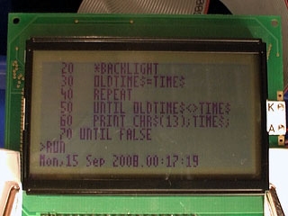
Finally, the obligatory video, this time showing a clock that toggles the backlight once a second.
Bank-Switching Memory and I2C
Thursday, 11th September 2008
Cheers for the comments.  As EasilyConfused pointed out, I have done calculator programming in the past, which makes this much easier - learning Z80 assembly to program a calculator influenced the choice of CPU in this computer, and porting BBC BASIC to the calculator showed that with a minimal amount of code to sit between it and the hardware you'd have a decent operating system with very little work. And if a Terminator-related name is good enough for the UK military, it should be good enough for this project...
The I/O board from a few posts ago has undergone a few revisions:
Both PS/2 ports are now fully wired up, though only the lower one is currently used by the OS for keyboard input. I will need to adjust the AT protocol routines (the AT protocol is used to control both keyboard and mouse) to support multiple physical ports, as it was adapted from code I wrote for the TI-83+ calculator and as such only supports one device at a time. The mouse position will be polled by calling ADVAL(axis%), which on the BBC Micro would return the joystick position (axis% specifies the type of information to retrieve from the mouse - a value of 0 returns the buttons as a bitfield, 1 returns the movement in the X axis, 2 the movement in the Y axis and 3 the amount the scrollwheel has been scrolled).
At the very bottom of the circuit board is another 8-bit latch. This is for the (currently) write-only control port. The three least significant bits specify the current ROM page (one of eight 16KB ROM pages can be swapped in for a total of 128KB) and the next bit specifies one of two 16KB RAM pages accessible in the $4000..$7FFF address range. One of the other bits will be used to switch the LCD backlight on and off in software, one more may be connected to a buzzer, and I'm sure I can find some use for the last two. As it's write-only, its current state needs to be stored in RAM so that you can change bits of it (eg when changing the ROM page you wouldn't want to change the backlight status at the same time; you'd need to retrieve the current state and mask in the bits you wish to preserve). This is obviously an ugly hack, and I'm hoping I'll be able to use some of the space to the right of the latch IC on the circuit board to add the other latch to allow the port to be read as well (an I/O port needs two latches - an output latch that takes data from the data bus and outputs it to external hardware, and an input latch that takes data from external hardware and puts it back on the data bus).
The first test of the new ROM paging hardware was to display a simple animation. Assuming 1KB on each ROM page was taken up by the animation playback program, that leaves 15KB per ROM page. A frame (128×64 pixels) is 1KB, so that's 15 frames per page, or 120 frames total. I converted a clip from Pink Floyd's Arnold Layne music video to a suitable format and wrote a playback routine that could run from RAM. When the computer booted it would copy the player to RAM and run it from there as it could then run uninterrupted when different ROM pages were swapped in to read the frame data.
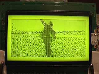
An animation like this is a useful test, as if the ROM paging didn't work properly (simulated by holding the three ROM page selection lines low) the software would still run, but would just loop the first 15 frames (or play chunks of 15 frames out of sequence) instead of crashing.
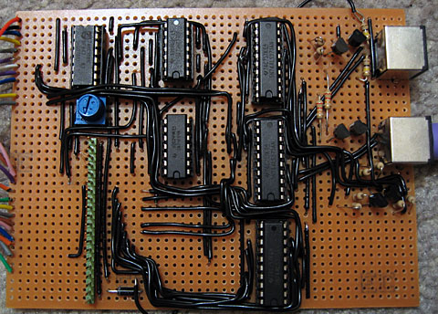
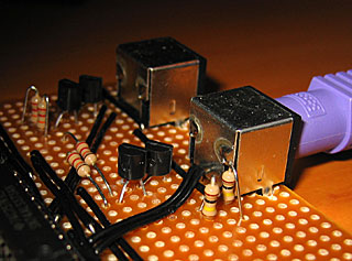
Another addition to the circuit above is the cluster of discrete transistors and resistors under the lowest PS/2 port. This is the same sort of pair of open-collector I/O data lines that drive each PS/2 port, except that the two data lines are fed out of the I/O board and back to the breadboard that's currently sitting between the memory board and the I/O board to these two simple 8-pin chips:
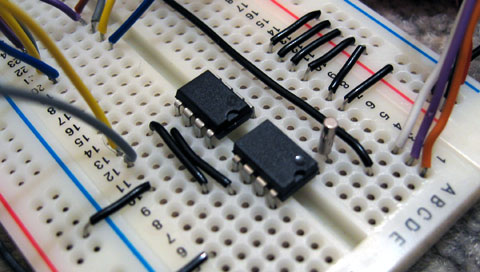
This is the I2C bus, a simple, low-speed, two-wire bus that will allow other components be easily connected to the computer. The I2C protocol is implemented in software. The two chips in the above image are a DS1307 real-time clock (foreground, with quartz crystal) which I hope to use for timing purposes and a 24LC256 32K×8 EEPROM which I hope to use for file storage. I would need to have some way of accessing the I2C bus externally (to plug in EEPROMs as removable storage) as well as supporting the internal devices.
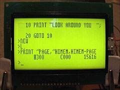
I haven't yet done any work on supporting I2C devices properly, but I have added I2C bus emulation to the emulator I'm using to develop the OS. BBC BASIC will pass commands prefixed with a *STAR to the operating system, so I've added a *I2CPROBE command that will hammer through all available addresses and list any devices that acknowledge a write request.
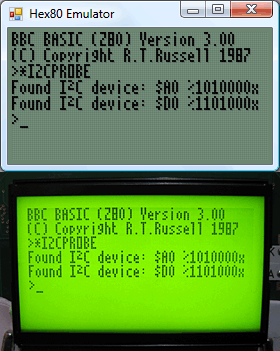
$A0 is the EEPROM and $D0 is the clock.
I think I may have dug myself into a hole for CPU timing. I mentioned that I will need to drop the CPU clock to 2MHz when accessing the LCD; unfortunately, switching between 2MHz and 10MHz doesn't seem to work very well. I can run the system relatively stably at either speed (though at 10MHz data sent to the LCD is occasionally corrupted) but if I try and switch dynamically (eg switching from the 10MHz to the 2MHz clock when /IORQ goes low to indicate an I/O request) the system locks up. My assumption is that during time it takes the logic gates that perform the 10MHz/2MHz switch to properly settle into their new state (which is in the tens of nanoseconds) the clock signal stutters a little, effectively producing a clock signal (albeit a brief one) well over 10MHz. I don't have an oscilloscope to verify this, however. 
Running BBC BASIC on a home-built computer
Sunday, 7th September 2008
This computer needs a name - I'd welcome any suggestions!
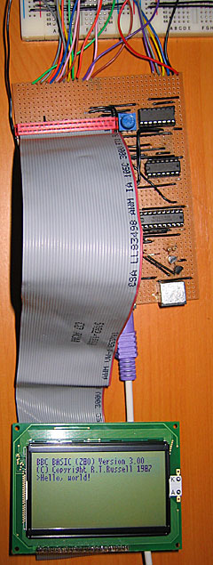
I have built a circuit on another piece of stripboard that will handle memory, clock signal generation and the Z80 itself.
A few posts ago I was wondering about how I'd partition memory. To date I've been using a very simple circuit where the lower 32KB of addressable memory is mapped to ROM and the upper 32KB is mapped to RAM. As my ROM chip is 128KB and I have two 32KB RAM chips, this seems a bit wasteful.
The memory layout I'm now using is quite simple: the upper 32KB is still mapped to RAM. However, only the first 16KB is mapped to ROM, and the three most significant bits of the ROM chip's address lines are connected to a device on the I/O board so that one of its eight 16KB "pages" can be swapped in. The next 16KB will be mapped to RAM, and the most significant bit of the RAM chip's address is connected to the same device on the I/O board so one of its two 16KB "pages" can be swapped in.
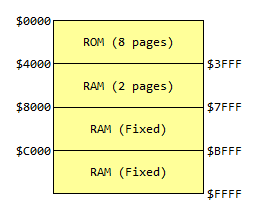
For more information, see the Wikipedia article on bank switching. There is a potential problem here; the Z80 uses particular fixed addresses for certain operations. The three most obvious ones are $0000 (jumped to on reset), $0038 (address of maskable interrupt handler) and $0066 (address of non-maskable interrupt handler). As which 16KB bank switched in at power-on is effectively random, the easy way around this problem is to ensure that the first 256 bytes or so of every ROM page has the same code assembled on it. This means that whichever page is swapped in on boot doesn't matter, as the same common boot code is available on each page.
The assembled memory board looks like this:
;if(img.style.backgroundImage){img.style.backgroundImage='url('+img.src+')';img.src=imgs[img.src.indexOf(imgs[1])<0?1:2]}else{img.style.backgroundImage='url('+img.src+')';img.src=imgs[2];};void(0);)
I have only attached one of the 32KB RAM chips. The wiring was becoming a bit of a nightmare (I think I'll need to solder to the track side of the stripboard to fit in that other RAM chip) so for the moment the system can only access the fixed 32KB RAM. I haven't yet added the device on the I/O board to handle bank switching, so for the moment the ROM is permanently configured to access the first 16KB page by pulling the its three externally controllable address lines low.
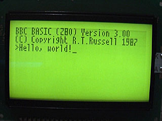
That said, this machine does genuinely run BBC BASIC (the last system only ran a mockup with a dummy header at the top of the screen). I've done quite a bit of work on the OS in the emulator and it works pretty well there, and with a minor adjustment to cram it onto a single 16KB page it works well on hardware too.
The row of chips along the bottom of the memory board are responsible for generating the clock signals that drive the computer. If this looks needlessly complex, that's because it can run at either 10MHz or 2MHz and generates the E signal for LCD access. The CPU needs to drop to 2MHz when accessing the LCD (the LCD driver can't keep up, otherwise) so I'll probably end up connecting the input for this 2MHz/10MHz switch to the LCD chip enable pins so that normally the system runs at 10MHz but drops to 2MHz when accessing the LCD. Allowing the user to drop to 2MHz to save power is an appealing idea, however...
2MHz should be enough for anyone
Wednesday, 27th August 2008
 LCD Timing
Last time I discussed the hardware I mentioned I had LCD timing issues. I have finally resolved them, but this has been the most time consuming part of the project so far.
The first thing to sort out was the LCD's E pin. Once you have set up the LCD's input pins to a state where they're ready to read or write data, you need to drive this pin high. I had had some success by holding it high permanently and relying on the Z80 to set all the other to the right state at roughly the same moment, but this was inaccurate and resulted in occasional display glitching.
Consulting the datasheet, it appears that once the input pins are ready E needs to be held low for at least 450nS and then needs to be driven high for at least 450nS. Hmm. During an I/O request (and once the Z80 has prepared the address and data bus) there's a delay of 1 clock cycle, then /IORQ is held low for about 2.5 CPU cycles. That is the window of opportunity. I have connected a binary counter to the Z80's clock signal and take the least significant bit of the output - every clock cycle this output toggles between a low and a low, effectively halving the CPU clock rate. I then connect the counter's reset pin (which overrides the clock input and forces it to output zero) to /IORQ. The result is that when the Z80 is not accessing hardware the counter is held in its reset state, and E is held low. When the Z80 holds /IORQ low, the counter starts up and outputs a zero for one CPU cycle, outputs a one for the next CPU cycle, then outputs a zero for the next half clock cycle at which point /IORQ goes high again and it is back to zero anyway. This is exactly what's needed!
This also allows us to calculate the maximum CPU clock rate. If we are generous and allow E to be low for 500nS then high for 500nS, that gives us a CPU clock rate of 1/500nS=2MHz.
Anyhow, that's one problem resolved, but there was still one nasty bug. When reading from the LCD it would occasionally end up writing to the area that was being read or, in worse cases, the Z80 would "crash". The LCD has a R/#W pin that is held high when reading and held low when writing. I had connected it directly to the Z80's /WR pin, which is high normally and low when writing. The problem here is "normally" as the LCD was expecting to be read even when the Z80 wasn't requesting a /RD. When being read, the LCD expects to put something onto the data bus, and it appeared that it kept thinking that it needed to put something on the bus when it wasn't needed. This caused fighting with the other chips that were trying to put their own values on the data bus, hence the crashes as the Z80 received invalid data.
The answer was very easy; simply connect the Z80's /RD pin to the LCD's R/#W pin via a NOT gate. In the default state the pin is held low (LCD expects a write and leaves the data bus alone), and only goes high during a /RD. The LCD interface is now very robust.
CPU Clock
Above I mention the calculation for the maximum clock rate. Rather than use the 555 for timing, I switched to using a 10MHz crystal resonator oscillator. I'm using the serial resonant circuit from z80.info with a 74F04 hex inverter (second circuit down). Fortunately the counter chips I have are decade counters (ie, designed to count from 0 to 9) made up of a ÷2 and a ÷5 section. I can connect a 10MHz oscillator to the ÷5 section and use the output of that to drive the CPU. In the final design I'd like to add a "hardware control port" with a bit that would let the programmer choose 2MHz or 10MHz mode by setting or resetting a particular output bit (other control bits would include switching the LCD backlight on or off and a buzzer for beeping sound output).
PS/2 Ports
As a friend pointed out, the 8-bit open-collector I/O port (which will drive two PS/2 ports, the I2C bus and TI calculator link port) had a flaw - there was no resistor on the base of the output transistors. The result is that if the output latch tries to drive the transistor base high, the transistor switches on and shorts the output of the latch to ground. This was clearly a problem in the design as the LCD backlight dimmed when trying to output to these ports as they drew a excessive amount of current when effectively short-circuited. A 22K resistor between the output latch and base of the transistor fixed the problem.
In the above photo, I've also added two 100K resistors to hold the output high when floating, but only to the foreground PS/2 port for the time being. I don't think I'll be controlling a mouse yet!
Revised OS
With a little modification of the Emerson PS/2 library I've got a basic keyboard driver up and running on the hardware. All the OS does for the moment is check for keys and display them on the screen. It's currently hard-coded to the UK layout, as I haven't yet decided how I'm going to handle storage and by keeping the layout in ROM it at least frees up a few hundred bytes of RAM that would otherwise need to be there for the scancode translation tables.
Remapped IO.DLL
Sunday, 24th August 2008
A common problem with software that uses the parallel port is that is hard-coded to use particular port addresses, such as 0x378 for LPT1. This is all well and good on older machines that have integrated or ISA ports that can be assigned this base address, but newer machines with PCI cards don't get any choice over which port address range is assigned to the parallel port.
The supporting software for the Willem programmer has this problem, and so far I've been using an old XP laptop with a flaky WiFi adapter to program chips. This has been rather painful, understandably!
Fortunately, in Windows NT Microsoft forbade us from accessing hardware ports directly when in user-mode. This probably doesn't sound very fortunate, but the result is that various libraries for accessing the I/O ports using an embedded kernel-mode driver sprang up. Whilst this still isn't perfect (you need to run the calling app with Administrator privileges) it does mean that apps that access the parallel port will have one of these libraries kicking around as a DLL in their installation directory. The Willem programmer software is no exception; it uses IO.DLL.
The trick, then, is to simply replace the IO.DLL bundled with the app with a custom one that performs the same task, but redirects port writes in the LPT1 range (0x378~0x37F) to a user-specified base address (in my case, 0xCCD8). I couldn't get IO.DLL itself to work from within a DLL, and using it meant that you'd have to also rename the existing IO.DLL to something else, so I used Inpout32.dll instead to access the ports from the new DLL.
IO.DLL provides many helper functions, Inpout32.dll only offers two - Inp32() and Out32(). Fortunately, the Willem software doesn't seem to use any of the helper functions, and only uses PortIn() and PortOut(). (It does also use IsDriverInstalled(), but I've hard coded that to always return -1). The sample C++ interface code doesn't check the return value of GetProcAddress(), so the software still initialises, but will crash with an access violation if it tries to use any of the unsupported functions.
With some help from ibutsu to get around the C function name mangling problem (resolved by adding a simple .def file), you can simply extract three files into the Willem software directory (new io.dll, inpout32.dll for port access and io.ini for the user-specified port address) and the software appears to work fine! (I haven't tested all chip modes, as I only have one type of flash memory chip and an I2C serial EEPROM, but they work).
Download DLLs and source or documentation.